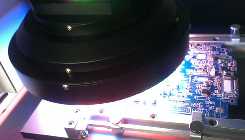
Automated optical inspection (AOI) is an automated visual inspection of printed circuit board (PCB) (or LCD, transistor) manufacture where a camera autonomously scans the device under test for both catastrophic failure (e.g. missing component) and quality defects (e.g. fillet size or shape or component skew). It is commonly used in the manufacturing process because it is a non-contact test method. It is implemented at many stages through the manufacturing process including bare board inspection, solder paste inspection (SPI), pre-reflow and post-reflow as well as other stages.
Historically, the primary place for AOI systems has been after solder reflow or “post-production.” Mainly because, post-reflow AOI systems can inspect for most types of defects (component placement, solder shorts, missing solder, etc.) at one place in the line with one single system. In this way the faulty boards are reworked and the other boards are sent to the next process stage
Post time: Sep-23-2020

